Find Power Bank OEM, Phone Power Bank , Powerbank on Industry Directory, Reliable Manufacturer/Supplier/Factory from China.

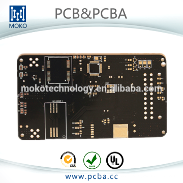
Model No.: MK50906BJ15
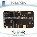
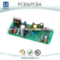
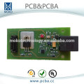
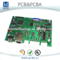
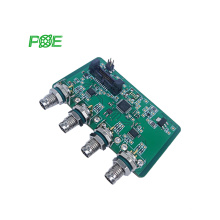
PCB&PCBA, Welcome to MOKO!

MOKO TECHNOLOGY LTD was founded in 2001, located in Shenzhen. We mainly offer GPS Tracker PCB Manufacturing and OEM PCB Assembly Service. From our ISO9001:2008 certified factory, we turn out up to 10000 square meter of PCBs and 400000 PCBAs monthly. For assembly, utilizing 8 high-speed SMT lines from Yamaha and Sony, to meet customers' need.
MOKO offer PCBA for kickstarters, engineering offices and global elctronic companies.
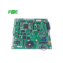
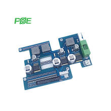
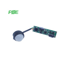
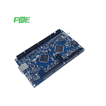
Our PCBA are apply for medical care devices; vending machine; GPS tracker; Smoke alarm; Food detector; Blood pressure instrument; fish finder; communication board and other fields.
Moko atended exhibitions,EXPO Munish 2012,2014; EXPO Moscow 2013,2015; HK Electronic Fairs.

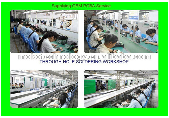
1)ROHS SMT WORKSHOP

2)High Standard Through-Hole Slodring Workshop
3)Good After Testing Service

4)PCBA production process

PCB Technical Specification
| Number of Layer | 1,2,4 or 6,upto 18 layer |
| Order Quantity | 1 to 50,000 |
| Board Shape | Retangular,round,slots,cutouts,complex,irregular |
| Board Type | Rigid, Flexible, Rigid-flexible |
| Board Material | FR-4 glass epoxy, FR-4 high Tg, Rohs compliant,Aluminum,Rogers,etc. |
| Board Cutting | Shear,V-score,Tab-routed |
| Board Thickness | 0.2-4.0mm, Flex 0.01-0.25mm |
| Copper Weight | 1.0, 1.5, 2.0 oz |
| Solder Mask | Double-sided green LPI,Also support Red,White,Yellow,Blue,Black |
| Silk Screen | Double-sided or single-sided in white,yellow,black,or negative |
| Silk Screen Min Line Width | 0.006'' or 0.15mm |
| Max Board Dimensions | 20 inch*20inch or 500mm*500mm |
| Min Trace/Gap | 0.10mm, or 4mils |
| Min Drill Hole Diameter | 0.01'',0.25mm, or 10mils |
| Surface Finish | HASL,Nickle,Immersion Gold,Immersion Tin,Immersion Silver,OSP,etc. |
| Board Thickness Tolerance | ±10% |
| Copper Weight Tolerance | ± 0.25 oz |
| Minimal Slot Width | 0.12'', 3.0mm, or 120mils |
| V-Score Depth | 20-25% of board thickness |
| Design File Formate | Gerber RS-274,274D,Eagle and AutoCAD's DXF,DWG |
PCBA Capabilities
| Quantity | Prototype&Low Volume PCB Assembly,from 1 Board to 250,is specialty,or up to 1000 |
| Type of Assembly | SMT,Thru-hole |
| Solder Type | Water Soluble Solder Paste,Leaded and Lead-Free |
| Components | Passive Down to 0201 size BGA and VFBGA Leadless Chip Carriers/CSP Double-sided SMT Assembly Fine Pitch to 0.8mils BGA Repair and Reball Part Removal and Replacement |
| Bare Board Size | Smallest:0.25*0.25 inches Largest:20*20 inches |
| File Formate | Bill of Materials Gerber files Pick-N-Place file |
| Types of Service | Turn-key,partial turn-key or consignment |
| Component packaging | Cut Tape,Tube,Reels,Loose Parts |
| Turn Time | Same day service to 15 days service |
| Testing | Flying Probe Test,X-ray Inspection AOI Test |
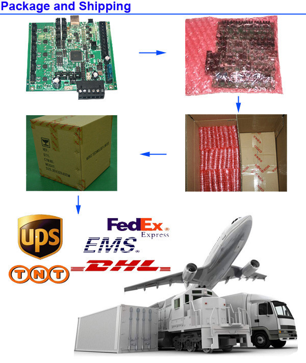
| PCB assembly process | Drilling-----Exposure-----Plating-----Etaching & Stripping-----Punching-----Electrical Testing-----SMT-----Wave Soldering-----Assembling-----ICT-----Function Testing-----Temperature & Humidity Testing |
PCB Lead time:
| Single/double side | 4 layer | 6 layer | Above 8 layer | HDI | |
| Sample lead time(Normal) | 5-6 | 6-7 | 7-8 | 10-12 | 15-20 |
| Sample lead time(Fastest) | 48-72 hours | 5 | 6 | 6-7 | 12 |
| Mass production lead time(First batch) | 7-9 | 10-12 | 13-15 | 16 | 20 |


Why us?
Quality
Our UL/Rohs standards insure quality assemblies from start to finish. Whether it's a simple custom product or a complex turnkey production run, Moko will adhere to the highest quality standards.
--------------------------------------------------------------------------------
Capable
Moko offers the latest in assembly capabilities and qualifications insuring that quality is built into every product we produce.
--------------------------------------------------------------------------------
Experience
When it comes to your build you want a partner you can depend on. Our management team has over 10years of combined industry knowledge. Our engineering team has over 7 years experience.
--------------------------------------------------------------------------------
Protecting your interests
Protecting your Intellectual Property is job one! Our staff of trained professionals are all working under a strict confidentiality contract and treat your important documentation as they would their own.
--------------------------------------------------------------------------------
Flexibility
We pride ourselves on our ability to custom tailor programs around our customers' needs. We take time to listen to your unique business needs and then set out to surpass them.

Q:What's files do you use in the bare board fabrication?
A:Gerber RS-274X,274D,Eagle and AutoCAD's DXF,DWG
Q: Will our PCB files be checked?
A: Yes. Your data will be checked by our Engineers Team. If we find any technical issues or have any enquires we will contact you and solve the problems together.
Q:What's files do you need in the PCBA projects?
A:Exclude the pcb file, the PNP(Pick and Place) file and Components Position file also needed.
Q: How can i know the processing about my PCB or PCBA order?
A: Each Customer will have a sale to contact with you. MOKO working hours:AM9:00-PM6:00(Beijing Time) from Monday to Friday. We will reply your email in 2 hours in our working time. And you also can contact with our sales's cell phone if urgent.
Q: Dose our product will be tested before shipment?
A: Yes, we could provide Function Circuit Testing if you provide us the testing methods.
Contact me:
Jacky Wang Sales engineer
Office: 086-0755-23573370-822 Cell: 086-18511247912
Skype: jacky19870314(at)outlook.com
Linkedin:?id=426044499&trk=nav_responsive_tab_profile
Web:
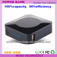
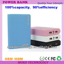
Product Categories : Power Bank OEM