Find Multi-layer PCB, Circuit Board , Printed Circuit Board on Industry Directory, Reliable Manufacturer/Supplier/Factory from China.
Model No.: MK41121BE01
2 layer commercial PCB sample production in 24 hours
PCB Technical Specification
| Number of Layer | 1,2,4 or 6,upto 18 layer |
| Order Quantity | 1 to 50,000 |
| Board Shape | Retangular,round,slots,cutouts,complex,irregular |
| Board Type | Rigid, Flexible, Rigid-flexible |
| Board Material | FR-4 glass epoxy, FR-4 high Tg, Rohs compliant,Aluminum,Rogers,etc. |
| Board Cutting | Shear,V-score,Tab-routed |
| Board Thickness | 0.2-4.0mm, Flex 0.01-0.25mm |
| Copper Weight | 1.0, 1.5, 2.0 oz |
| Solder Mask | Double-sided green LPI,Also support Red,White,Yellow,Blue,Black |
| Silk Screen | Double-sided or single-sided in white,yellow,black,or negative |
| Silk Screen Min Line Width | 0.006'' or 0.15mm |
| Max Board Dimensions | 20 inch*20inch or 500mm*500mm |
| Min Trace/Gap | 0.10mm, or 4mils |
| Min Drill Hole Diameter | 0.01'',0.25mm, or 10mils |
| Surface Finish | HASL,Nickle,Immersion Gold,Immersion Tin,Immersion Silver,OSP,etc. |
| Board Thickness Tolerance | ±10% |
| Copper Weight Tolerance | ± 0.25 oz |
| Minimal Slot Width | 0.12'', 3.0mm, or 120mils |
| V-Score Depth | 20-25% of board thickness |
| Design File Formate | Gerber RS-274,274D,Eagle and AutoCAD's DXF,DWG |
PCBA Capabilities
| Quantity | Prototype&Low Volume PCB Assembly,from 1 Board to 250,is specialty,or up to 1000 |
| Type of Assembly | SMT,Thru-hole |
| Solder Type | Water Soluble Solder Paste,Leaded and Lead-Free |
| Components | Passive Down to 0201 size BGA and VFBGA Leadless Chip Carriers/CSP Double-sided SMT Assembly Fine Pitch to 0.8mils BGA Repair and Reball Part Removal and Replacement |
| Bare Board Size | Smallest:0.25*0.25 inches Largest:20*20 inches |
| File Formate | Bill of Materials Gerber files Pick-N-Place file |
| Types of Service | Turn-key,partial turn-key or consignment |
| Component packaging | Cut Tape,Tube,Reels,Loose Parts |
| Turn Time | Same day service to 15 days service |
| Testing | Flying Probe Test,X-ray Inspection AOI Test |
| PCB assembly process | Drilling-----Exposure-----Plating-----Etaching & Stripping-----Punching-----Electrical Testing-----SMT-----Wave Soldering-----Assembling-----ICT-----Function Testing-----Temperature & Humidity Testing |
Technical requirement for pcb&pcb assembly:
1. Professional Surface-mounting and Through-hole soldering Technology
2. Various sizes like 1206,0805,0603 components SMT technology
3.ICT(In Circuit Test),FCT(Functional Circuit Test) technology.
4.PCB Assembly With UL,CE,FCC,Rohs Approval
5.Nitrogen gas reflow soldering technology for SMT.
6.High Standard SMT&Solder Assembly Line
7. High density interconnected board placement technology capacity.
Quotation requirement for pcb&pcb assembly:
1. PCB gerber file
2. BOM list for PCBA
3. Sample of PCB and PCBA
4.Test method for PCBA
Lead time:
PCB | Single/double side | 4 layer | 6 layer | Above 8 layer | HDI |
Sample lead time(Normal) | 5-6 | 6-7 | 7-8 | 10-12 | 15-20 |
Sample lead time(Fastest) | 48-72 hours | 5 | 6 | 6-7 | 12 |
Mass production lead time(First batch) | 7-9 | 10-12 | 13-15 | 16 | 20 |
PCB Assembly | PCB Fab+Components Sourcing+PCBA=20 days | ||||
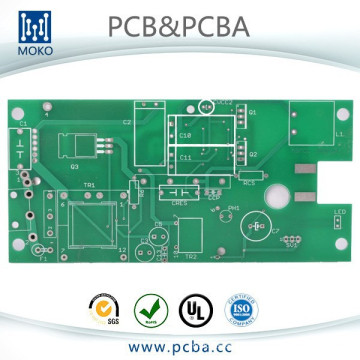
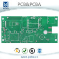
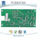
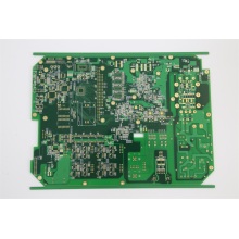
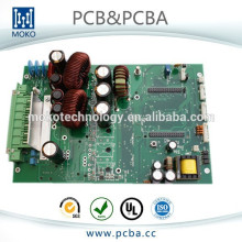
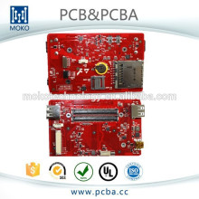
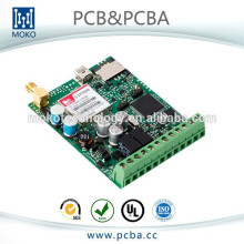
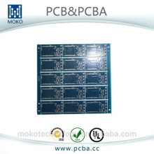
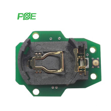
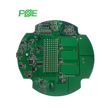
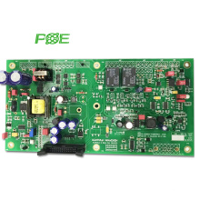
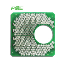
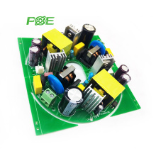
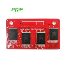
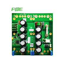
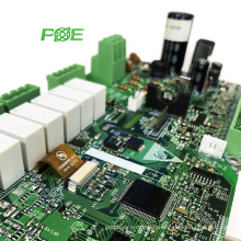
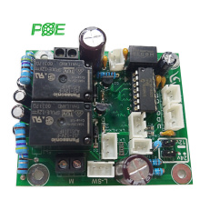
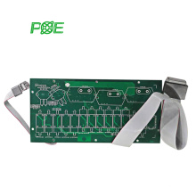
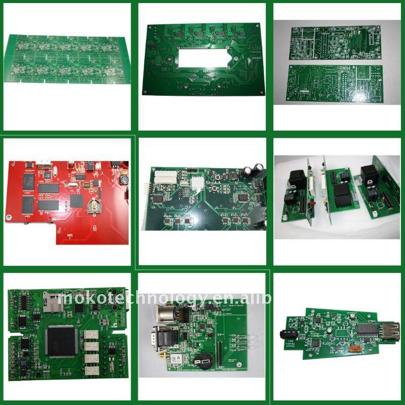
relating product show
Inner Carton:

Outer Carton:

1.PCB
2.Component service
3.PCB Assembly
4.PCBA testing

Q: What files do you use in PCBA fabrication?
A: Gerber or Eagle, BOM listing, PNP and Components Position
Q:Is it possible you could offer sample?
A: Yes, we can custom you sample to test before mass production
Q: When will I get the quotation after sent Gerber, BOM and test procedure?
A: Within 6 hours for PCB quotation and around 24 hours for PCBA quotation.
Q: How can I know the process of my PCBA production?
A: 7-10 days for PCB production and components purchasing, and 10 days for PCB assembly and Testing
Q: How can I make sure the quality of my PCBAs?
A: We ensure that each piece of PCBA products work well before shipping. We'll test all of them according to your test procedure. Also if there are any defect items during the shipping, we also can be free to repair for you.
Contact us if you need more details on Commercial Pcb. We are ready to answer your questions on packaging, logistics, certification or any other aspects about Pcb Sample Production、2 Layer Pcb. If these products fail to match your need, please contact us and we would like to provide relevant information.
Product Categories : Multi-layer PCB