Find Multi-layer PCB, Circuit Board , Printed Circuit Board on Industry Directory, Reliable Manufacturer/Supplier/Factory from China.
Model No.: MK2013HH069
Welcome To Moko
MOKO TECHNOLOGY LTD was founded in 2001, located in Shenzhen. We mainly offer Electronics Assembly Service. From our ISO9001:2008 certified factory, we turn out up to 10000 square meter of PCBs and 400000 PCBAs monthly. For assembly, utilizing 8 high-speed SMT lines from Yamaha and Sony, to meet customers' need.
Moko, your single point of contact for all of your raw materials, parts, and PCB Assembly, also offers: - Contract Manufacturing
- Engineering Services
- Pcb Design & Assembly
- Product Design
- Prototyping
- Cable and Wire Assemblies
- Plastics and Molds
1.Detailed Specification of PCB Board Manufacturing
| 1 | Layer | 1-30 layer |
| 2 | Material | FR-4,CEM-1,CEM-3,Hight TG,FR4 Halogen Free,FR-1,FR-2,Aluminum |
| 3 | Board thickness | 0.2mm-7mm |
| 4 | Max.finished board side | 800mm*500mm |
| 5 | Min.drilled hole size | 0.25mm |
| 6 | Min.line width | 0.075mm(3mil) |
| 7 | Min.line spaceing | 0.075mm(3mil) |
| 8 | Surface finish/treatment | HASL/HASL lead free,Chemical tin,Chemical Gold,Immersion gold Inmersion Silver/Gold,Osp,Gold Plating |
| 9 | Copper thickness | 0.5-4.0oz |
| 10 | Solder mask color | green/black/white/red/blue/yellow |
| 11 | Inner packing | Vacuum packing,Plastic bag |
| 12 | Outer packing | Standard carton packing |
| 13 | Hole tolerance | PTH:±0.076,NTPH:±0.05 |
| 14 | Certificate | UL,ISO9001,ISO14001,ROHS,CQC |
| 15 | Profiling Punching | Routing,V-CUT,Beveling |
| 16 | Assembly Service | Providing OEM service to all sorts of printed Circuit Board Assembly |
2.Detailed Terms for Pcb Assembly
Technical Requirement for pcb assembly:
1) Professional Surface-mounting and Through-hole soldering Technology
2) Various sizes like 1206,0805,0603 components SMT technology
3) ICT(In Circuit Test),FCT(Functional Circuit Test) technology.
4) PCB Assembly With UL,CE,FCC,Rohs Approval
5) Nitrogen gas reflow soldering technology for SMT.
6) High Standard SMT&Solder Assembly Line
7) High density interconnected board placement technology capacity.
Production Requirement for pcb assembly:
1.Gerber Files (Eagle and PCB File are available).
2.BOM list.
3.Clear pictures of PCBA or PCBA samples to us.
4.Pick N Place file.
5.Test procedure for PCBA.
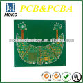
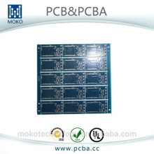
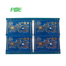
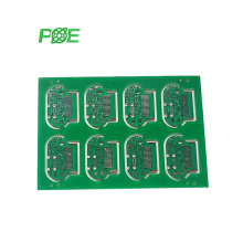
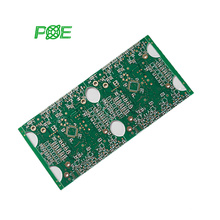
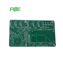
3.View of MOKO PCB

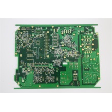
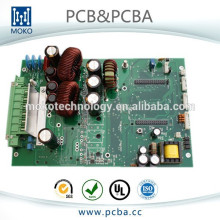
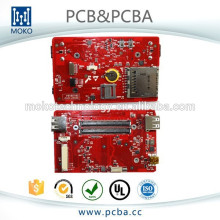
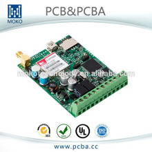
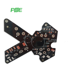
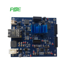
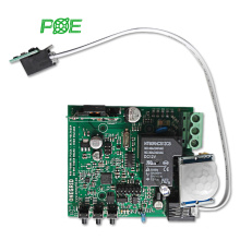
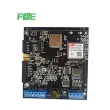
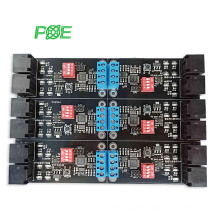
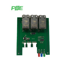
4.View of MOKO PCBA

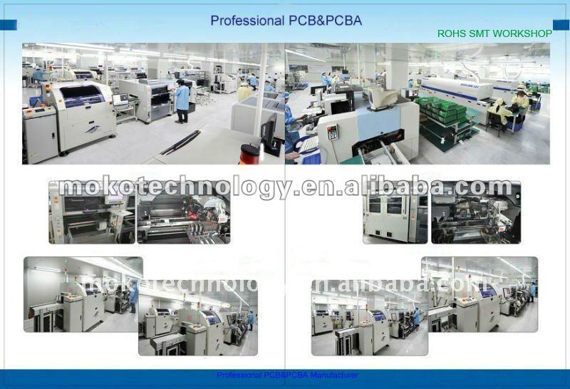
5.View of MOKO Factory
1)ROHS SMT WORKSHOP
2)High Standard Through-Hole Soldering Workshop

3)All goods after Testing Service

Q: What files do you use in PCB fabrication?
A: Gerber RS-274X, 274D, Eagle and AutoCAD's DXF, DWG.
Q:What format of BOM do you prefer?
A: We prefer to Excel with components part number, manufacturer, quantity, value information. Of course, other format is ok.
Q: How long will your quotation be sent after I sent Gerber, BOM and test procedure?
A: For PCB, our quotation will be sent within 6 hours. For PCBA, it's 2 working days. As for some special components, you could recommend suppliers to us.
Q: How can I know the process about my PCBA order?
A: Each customer will have a sale to contact. We'll email you about the process. You also could contact us by cell phone in urgent.
Q: Will all PCBAs be tested before delivery?
A: Yes, we ensure that each piece of PCBA products work well before shipping. We'll test all of them according to your test procedure. What you get from MOKO is high quality product.
Contact us if you need more details on Custom Circuit Board. We are ready to answer your questions on packaging, logistics, certification or any other aspects about Solder Resist Mask Pcb、Pcb with Blue Mask. If these products fail to match your need, please contact us and we would like to provide relevant information.
Product Categories : Multi-layer PCB